
Microscopes
Confocal Laser Scanning Microscopy
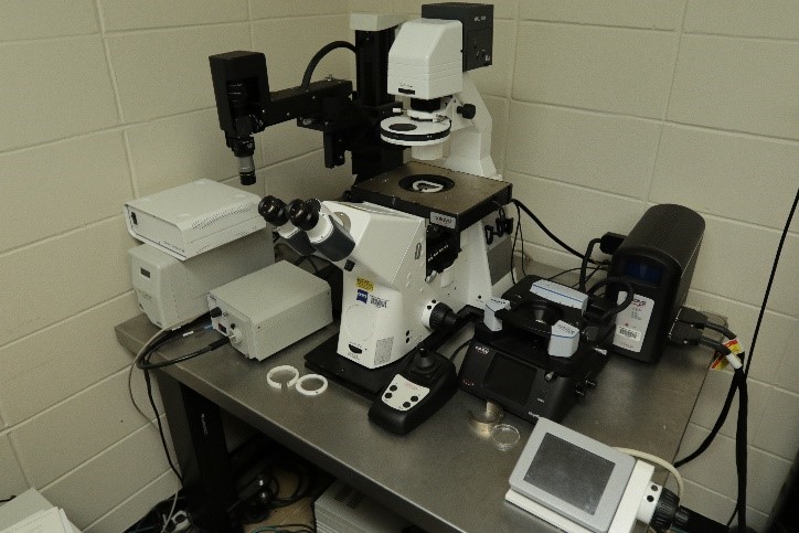
Axiovert 200 M Inverted Research Microscope
- 3 Confocal detection channels
- Laser lines [nm]
- 405 Diode 30 MW
- Argon multiline (458/477/488/514 30 MW)
- 543 HeNe 10 MW
- 594 HeNe 2 MW
- 633 HeNe 5 MW
- Objectives: "Type" magnification/numerical aperture, Working Distance
- "Plan Apochromat" 5x/0.16, WD=12.1
- EC "Plan Neofluar" 10x/0.30, WD=5.60
- "Plan-Apochromat" 20x/0.80, WD=0.55
- EC Plan "Neofluar" 40x/1.30 Oil DIC, WD=0.20
- "C-Apochromat" 40x/1.20 W corr, WD=0.28
- "Plan-Apochromat" 63x/1.40 Oil DIC, WD=0.18
- "Plan-Apochromat" 100x/1.40 Oil DIC, WD=0.17
- Mercury light source for fluorescence viewing
Atomic Force Microscopes
An atomic force microscope is a type of high resolution scanning probe microscope that
has a resolution that you can measure in fractions of a nanometer.
More detailed information on Atomic Force Microscopy can be found here:
The Atomic Force Microscope (AFM), What are its Uses in Microscopy Today
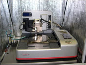
Dimension Icon AFM with ScanAsyst
- Resolution: ~nm range and possible ~Am
- XY piezo: 90 micrometers
- Z piezo: 10 micrometers
- Capabilities:
- PeakForce Tapping
- Contact mode
- Tapping mode
- MFM (Magnetic force microscopy
- Electricity:
- CAFM (conductive AFM)
- EFM (Electrostatic force microscopy)
- KPFM (Kelvin Probe force microscopy)
- PeakForce Tuna (PeakForce Tunnelling AFM)
- EC-AFM (Electrochemical AFM)
- IV curve
- PeakForce QNM (PeakForce Quantitative Naomechanics):
- Young’s modulus
- Reduce modulus
- Stiffness
- Adhesion
- Deformation
- Dissipation
- Nanolithography
- Temperature range: -50 ~ 250 C
BioScope Catalyst AFM with ScanAsyst
- Resolution: ~nm range
- XY piezo: 150 micrometers
- Z piezo: 15-20 micrometers
- Capabilities:
- PeakForce Tapping
- Contact mode
- Tapping mode
- MFM (Magnetic force microscopy
- EFM (Electrostatic force microscopy)
- PeakForce QNM (PeakForce Quantitative Nanomechanics):
- Young’s modulus
- Reduce modulus
- Stiffness
- Adhesion
- Deformation
- Temperature Range: ~40 C
- The Microscope Image Registration and Overlay (MIRO™) feature automatically imports and rescales light microscope images, allowing them to be used to direct the location of AFM imaging and force measurements
Scanning Electron Microscopes
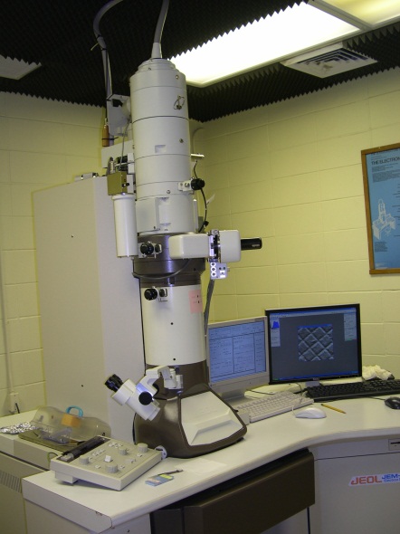
JEOL 6500F Field Emission SEM
- 'Video Classroom' equipped for two-way interactive communications with remote sites via the Internet
- Backscattered and secondary electron detectors
- Digital image storage
- With attached X-EDS spectrometer and Oxford Instruments INCAEnergy+ software
for electron beam-induced X-ray elemental analysis
- with ultra-thin window (for boron and higher atomic number element detection)
- With attached EBSD detector and Oxford Instruments INCA Crystal software for Electron Backscatter Diffraction (EBSD) crystallographic analysis
- Maintained on service contract
- Resolution on secondary electron image:
- 1.5 nm (at accelerating voltage 15kV)
- 5.0 nm (at accelerating voltage 1kV)
- Accelerating voltage: 0.5 to 30 kV
- Magnification range: 10X to 500,000X
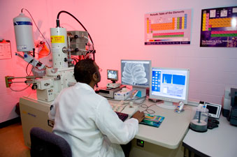
The JEOL 6500F Field Emissions SEM
HITACHI TM-1000 Table-Top SEM
- Easy to use
- Depth of Focus: 0.5mm
- Resolution: 30nm
- Magnification Range: 20-10,000
- Sample Size: Up to 70mm
- Stereoscopic
- Available for Outreach
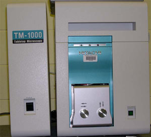
The HITACHI TM-1000 Table-Top SEM
Transmission Electron Microscopes
JEOL 1230 120kV TEM
- Tungston emitter
- Accelerating voltage - 80 kV
- Resolution: Point: .36 nm Lattice: .2 nm
- Bottom mount Gatan Camera with Digital Micrograph Software
- Single tilt holder
- Based on MS Windows™ software
- High-stability goniometer stage
- 5 spot sizes
The JEOL 1230 120kV TEM
JEOL 2100 200kV TEM
- LaB6 emitter
- Accelerating voltage - 80,100,120,160,200 kV
- Resolution: Point: 0.23 nm, Lattice: 0.14 nm
- Oxford EDS system for elemental analysis and mapping
- Bottom and side mount Gatan Cameras with Digital Micrograph Software
- Double and single tilt holders
- Based on MS Windows™ software
- High-stability goniometer stage and the highest probe current for any given probe size, which allows for improved analytical and diffraction capabilities. The patented JEOL Alpha Selector™ allows a user the selection of a variety of illumination conditions, ranging from full convergent beam to parallel illumination