
Scanning Electron Microscope
A scanning electron microscope (SEM) is an advanced imaging tool that
uses a focused electron beam to produce high-resolution images of surface
morphology, revealing micro- and nano-scale features while also enabling
elemental and material analysis. Our current SEM capabilities include
nanometer to sub-nanometer resolution imaging and analysis of a wide
range of samples—including beam-sensitive and non-conductive
materials—often without the need for conductive coating. Integrated
energy dispersive X-ray spectroscopy (EDS) allows for seamless elemental
mapping and compositional analysis.
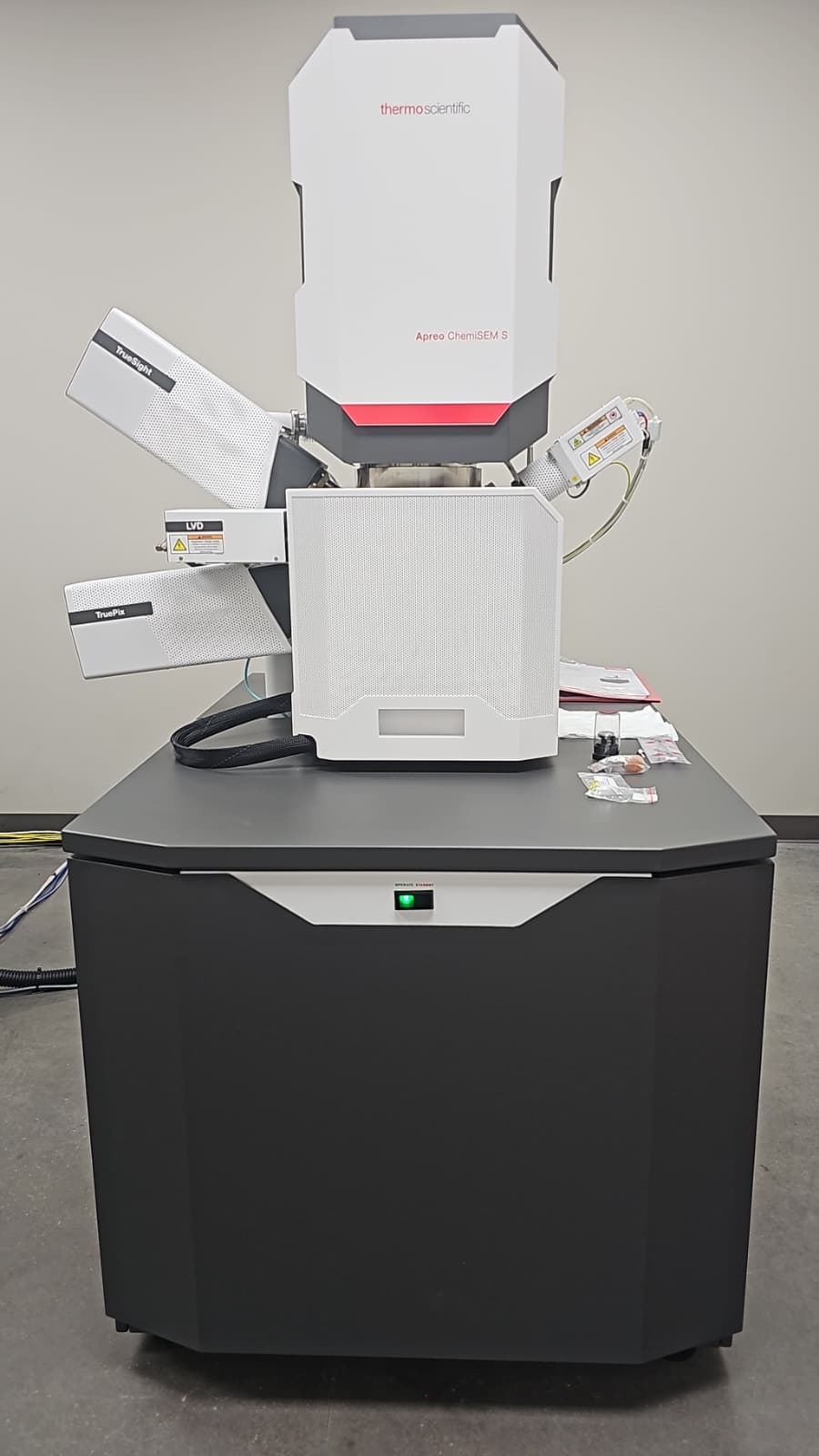
Apreo 2 SEM
The Apreo 2 Scanning Electron Microscope was acquired through the U.S. National Science Foundation (NSF) Major Research Instrumentation (MRI) Program (Award DMR-2510038).
Resources:
Specifications:
The Apreo 2 Scanning Electron Microscope was acquired through the U.S. National Science Foundation (NSF) Major Research Instrumentation (MRI) Program (Award DMR-2510038).
Resources:
Specifications:
| Resolution |
- 0.9 nm at 1 kV - 0.8 nm at 1 kV (beam decel.) - 1.0 nm at 1 kV, 10 mm working distance (beam decel.) - 0.8 nm at 500 V (beam decel.) - 1.2 nm at 200 V (beam decel.) |
| Standard Detectors | ETD, T1, T2, T3, IR-CCD, Nav-Cam+ |
| PivotBeam | Mode for selected area electron channeling (also known as "rocking beam" mode) |
| Optional Detectors | DBS, LVD, STEM 3+, EDS, EBSD |
| ChemiSEM Technology | Live quantitative SEM image coloring is available based on energy dispersive X-ray spectroscopy (EDS). Point & ID, linescan, region, element maps, and reliable Noran quantification are included. |
| Landing Energy Range | 20 eV – 30 keV |
| Stage Bias (Beam Deceleration) | -4000 V to +600 V standard with every system |
| Low Vacuum Mode | Optional: 10 – 500 Pa chamber pressure |
| Stage | 5-axis motorized eucentric stage, 110 x 110 mm2 with a 105° tilt range. Maximum sample weight: 5 kg in un-tilted position. |
| Maximum Beam Current | 50 nA |
| Standard Sample Holder | Multi-purpose holder, uniquely mounts directly onto the stage, hosts up to 18 standard stubs (Ø12 mm), three pre-tilted stubs, cross-section samples and two pre-tilted row-bar holders (38° and 90°) and does not require tools to mount a sample |
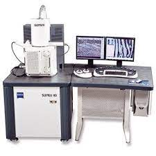
Zeiss SUPRA 40
Resources:
Specifications:
Resources:
Specifications:
| Nominal Resolution | 1.5 nm (at accelerating voltage 10kV) |
| Accelerating Voltage | Max. 30kV |
| Magnification Range | 10X to 500,000X |
| Attachments | EDAX EBSD with OIM software |
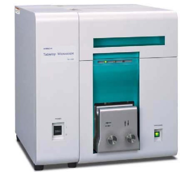
Hitachi TM-1000 Table Top SEM
Specifications:
Specifications:
| Depth of Focus | 0.5mm |
| Resolution | 30nm |
| Magnification Range | 20-10,000X |
| Sample Size | Up to 70mm |